")

Electrical discharges creating “cold” plasmas are today widely used for material processing in various fields including microelectronics, Microsystems, flat panel displays, and solar cells. Plasmas are used for material deposition, surface modification, or material removal (etching) especially anisotropic etching to create micro and nanostructures following a lithographic process. Fabrication of random or periodic nanostructure arrays (such as nanodots (0-d), perpendicular or parallel to the substrate nanowires (1d), and nanosheets or nanocurtains (2d)) on surfaces is extremely useful in many fields ranging from Life Sciences to Electronics and Photovoltaics. Perpendicular to the substrate nanowires (i.e. high aspect ratio nanopillars as we will refer to in this proposal) are among the most popular 1d nanostructures for applications. Bottom-up, wet or dry fabrication methods are used to create such nanostructures from vapour or liquid phase with or without catalyst seeds [Barth, Prog. Mat. Sci. 2010]. However, plasma nanofabrication is advantageous over bottom-up methods in that it is an environmentally friendly, fast, easily implemented technology, and typically produces well ordered nanopillars without the need of catalysts: Typically plasma nanofabrication uses anisotropic plasma etching, following top-down pattern definition on an intermediate polymeric layer (photoresist) using costly nanolithographic processes. The top-down approach is used today in the manufacturing of nanoelectronic and nanophotonic devices. On the other hand, self-assembly processes using specialty materials (such as block copolymers or colloidal nanoparticle suspensions to name only a few) are cost effective alternatives to lithography, and can be followed by plasma etching to transfer the pattern. This means that plasma etching can also be combined with bottom-up methods. We (and others) have recently used colloidal nanoparticle self-assembly to hexagonally assemble particles of a few hundred nm on surfaces of silicon and polymers. After isotropic plasma shrinking of the nanoparticles, anisotropic plasma etching followed to create nanopillars on the surface of Silicon and polymers [Ellinas, Microelec. Eng. 2011], [Ellinas, Langmuir 2011] resulting in superoleophobic surfaces. The same method has been used for nanostructured Si solar cells [Garnett, Annu. Rev. Mater. Res. 2011]. The method however, has problems of scalability and multiple layer packing, to name only a few. Thus, alternative methods for smaller nanopillars are necessay.
Could the plasma itself direct the formation of random or ordered nanostructures on the surfaces of processed substrates, i.e. could the plasma form the pattern and transfer it? This is the subject of the new field of plasma nanoscience and nanotechnology [Plasma Nanoscience special issue J. Phys. D 2011], [Plasma Nanoassemblies special issue J. Phys. D 2007]. This technology has only recently emerged as lithography-less nanofabrication route for 0d, 1d, 2d nanostructures with distinct advantages over other dry or wet methods. It is claimed that plasma nanofabrication mimics nature in the creation of the cosmos by “plasma nanoassembly” [Ostrikov, IEEE Trans. Plasma Sci. 2007], and that if used in the lab a “plasma nanofactory” will result. Among the various cutting-edge applications of plasma NanoScience are Nanoelectronics (graphene, carbon nanotubes), Energy (Silicon, hybrid, and organic photovoltaics-PVs, OPVs, other energy conversion routes, energy storage), and Health and environment [Ostrikov-Cvelbar-Murphy, J. Phys. D. 2011].
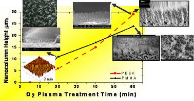
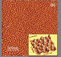
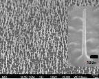
One way to create random nanopillars is to roughen a surface during anisotropic etching: We have observed the creation of extremely tall, random, pillar-like roughness formation on plasma etched polymer, which we coined as “nanotexture” (see fig. 1a). We have created both organic and silicone-rubber such random nanopillars, and we have exploited them for creating superhydrophobic polymeric surfaces [Tserepi, Nanotech. 2006], [Vourdas, Nanotech. 2007]. Recently, while experimenting with various etching conditions, we have also discovered that plasma etching can be used to direct the assembly of 20-100nm ordered, periodic dots on any polymeric surface or film, under appropriate etching conditions. This was a striking and unexpected new result. Using such polymeric nanodots as a mask, we subsequently etched Si creating ordered Si nanopillars [Vourdas, Nanotech. 2010] (see Fig. 1b,c). We have also discovered that the mechanism of random and ordered plasma nanoassembly is the simultaneous to etching deposition of a small amount of etch inhibitors from the plasma-reactor walls [Tsougeni, Langmuir 2009], [Vourdas, Nanotech. 2010]. We therefore have demonstrated the potential of subtractive plasma nanoassembly in mimicking top-down nanofabrication in a totally bottom-up approach [Gogolides, J. Phys. D. 2011]. Our results thus far are a paradigm shift in the use of processing plasmas, and show the potential of plasma nanoscience and nanotechnology. This proposal, which we will coin “plasma-NanoFactory”, concerns the further development of this field, aiming on one hand on the control of the process via control of the plasma-wall interactions and inhibitor flux, and on the other hand in applications in Life Sciences and Energy.
|
|
|
|
|
Fig.1 Plasma Nanoassembly: a) Random Nanotexturing of polymers with Plasmas: Oxygen plasma chemistry is used for organic polymers, such as PMMA, PEEK, PET, PS. Fluorine chemistry is used for Poly (dimethyl) siloxane (PDMS). High Aspect Ratio random nano and micro pillars are created. [Vourdas, Nanotech. 2007], [Tsougeni, Langmuir 2009], [Tserepi, Nanotech. 2006]. (b) AFM image (2x2 um2) of PMMA film surface after 46 s Oxygen plasma etching down to Silicon substrate. Notice the ordered nanodot assembly formation. RMS is ~5.2 nm. A 3D zoomed view of a part of the image is embedded [Vourdas, Nanotech. 2010]. c) Top down SEM view of a forest of Silicon nanopillars etched with SF6/O2 plasmas at -100 C. The mask was an array of oxygen-plasma-organized PMMA nanodots (see Fig. 3b). (aspect ratio 20:1, see zoomed nanopillars) (unpublished results) |
||