")

What is PlasmaNanoFactory or Plasma Nanofactory or Plasma Nano-Factory ?
Plasma etching is used to fabricate 0d, 1d, 2-dimensional nanostructures for a broad range of applications ranging from Nanoelectronics to Life Sciences. Plasma etching is used in a top-down approach, following expensive lithographic pattern definition. Recently, self-assembly of a pattern followed by plasma etching has been proposed as a cost-effective alternative to lithography. Could the plasma itself assemble the pattern and transfer it on a substrate? This is one of the topics of the new field of plasma nanoscience and of this project. In PlasmaNanoFactory, subtractive plasma nanoassembly, which comprises plasma etching with simultaneous deposition of etch inhibitors, is proposed as a method for high- aspect-ratio nanostructure fabrication, in a cost effective lithography-less manner. Plasma Nanoassembly as well as self-assembly followed by plasma.
Project results
Abstract
PlasmaNanoFactory is a project focusing on understanding and controlling plasma directed assembly (or else plasma nanoassembly) for nanostructure fabrication, and showing its potential in Life Science and Energy applications.
To achieve controlled plasma nanoassembly we needed to master the mechanism of plasma nanoassembly on polymeric substrates, and to design two new plasma sources for low pressure as well as atmospheric pressure. Indeed, we achieved for the first time controlled random nanostructure fabrication, and developed prototype equipment capable of performing such processes.
We used these surfaces for Life Science applications, and have made a groundbreaking discovery: We found out that cancer cells are preferentially enriched on such surfaces from their mixture with normal cells, a phenomenon, which may aid diagnostics and lab biopsy practices targeting cancer cell enrichment for early cancer diagnosis.
We have also nanostructured Silicon photovoltaics, as well as organic photovoltaics and have found encouraging efficiencies.
Work package 1: Controlling Plasma Nanoassembly
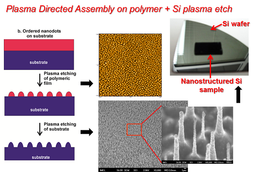
In WP1 the mechanism of plasma nanoassembly was studied for the formation of random and quasi ordered nanostructures on polymers. We proved that plasma etching with simultaneous deposition of etching inhibitors is the main mechanism of roughness formation. Such inhibitors may originate from sputtering of walls and electrodes in contact with the plasma. To control these effects new plasma sources were developed in this project.
In WP1 a new inductive plasma source was fabricated incorporating successively 4 antennas (Fig. 1a). Oxygen plasma etching with the new source showed impressive plasma nanotexturing and nanoassembly results for all 4 antennas. Control of sputtering from walls was achieved by shielding the local electric fields. Control of the geometry of random nanostructures was obtained via control of the amount of shielding of the electric fields. On the other hand, bias voltage, and temperature were used as control parameters for the quasi-ordered nanostructures. Two patents are being written for the new source and the new shielding approaches.
In addition to vacuum sources, the project addressed the need for atmospheric pressure uniform and large area plasma processing. A novel atmospheric plasma source was developed and patented (Fig. 1c).
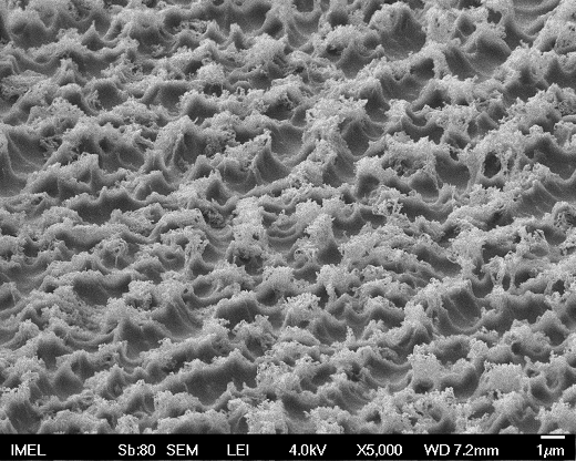
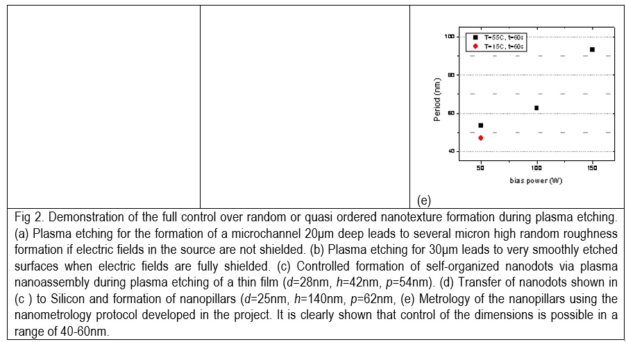
The design of the sources and shields was supported by electromagnetic simulation using electromagnetic simulation tools (Fig. 1b). Nanostructure morphology was visualized via SEM and AFM images. Such images were analyzed using a novel nanometrology protocol developed in the project using holistic metrology and fractal/scaling theory.The new plasma sources, as well as the nanometrology software have a great commercialization potential.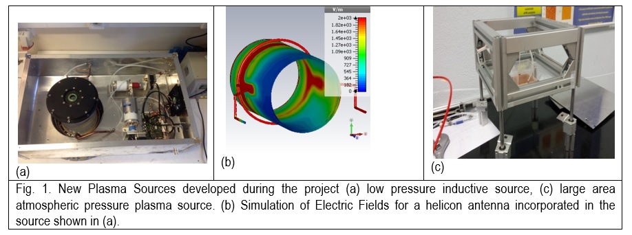
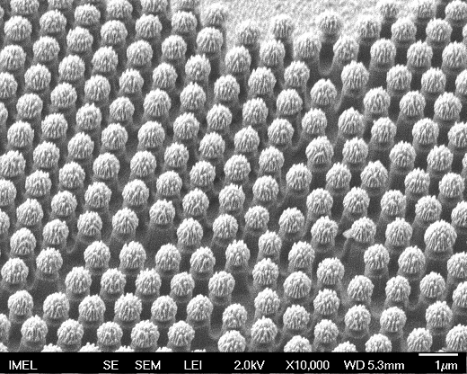
For the first time, using the new source and the new shielding developed in the project we achieved complete control of the nanotexture formation during plasma etching as seen in Fig. 2a,b for random nanostructures. In addition control of the dimensions of quasi ordered nanostructures was also achieved (see Fig. 2c,e) on polymers, as well as on Silicon (see Fig. 2d) by transferring the nanodots formed on Silicon.
Work package 2: Applications of PlsmaNanoFactory in Life Sciences
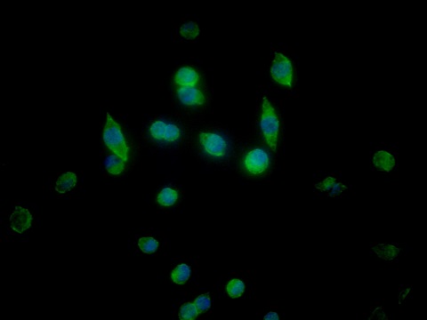
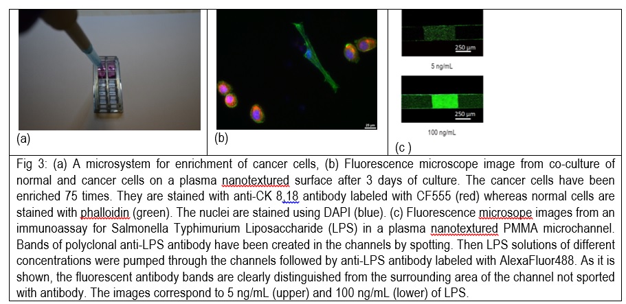
In WP2 experiments for normal and cancer cell attachment on rough plasma nanotextured surfaces showed significantly higher attachment and proliferation of cancer cells compared to normal cells, improving their enrichment ratio by at least a factor of 100. A simple microsystem for separation and enrichment of cancer cells from mixtures with healthy ones was therefore proposed (see Fig. 3a,b). In addition, in WP2 we fabricated a polymeric lab on chip for biomolecule separation using plasma nanotextured microfluidics (see Fig. 3c). To exploit the project findings a patent for rare cell enrichment was filed in Greece and EPO.
Work package 3: Applications of PlsmaNanoFactory in Energy
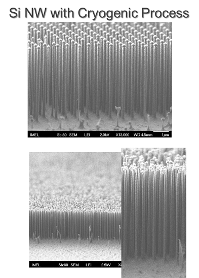
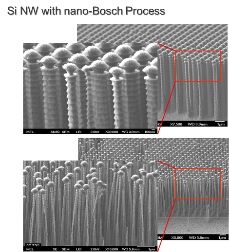
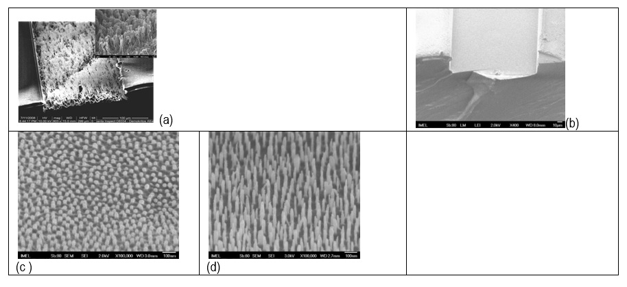
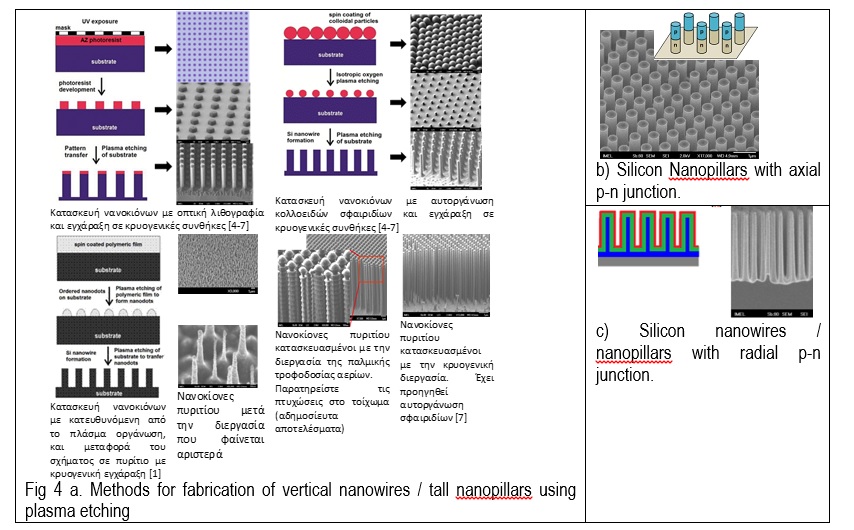
In WP3 we developed several process schemes for fabrication of Silicon nanopillars and nanowires (see Fig. 4a). Subsequently, photovoltaic devices were fabricated incorporating Si Nanowires (nanopillars) with axial or radial p-n junction (see Fig. 4b,c) and were characterized optically and electrically. Very encouraging results in terms of efficiency were obtained. Additionally, in WP3 plasma etching and nanotexturing of P3HT an organic semiconductor was done in oxygen plasmas. Significant differences in crystallinity, morphology, and optical properties were seen, also affecting (improving) the electrical characteristics. However, when organic photovoltaic devices were made incorporating the nanostructured P3HT, despite the higher open circuit voltage, loss of efficiency was observed (see Table 1). It was therefore concluded that direct plasma nanotexuring of organic photovoltaics is not the method to nanostructure their surfaces, but instead the technology should be used for indirect nanostructuring e.g. stamping.
|
Sample |
Jsc (mA/cm2) |
Voc (V) |
FF |
PCE (%) |
|
Reference Device |
-3.43 |
0.33 |
0.34 |
0.52 |
|
plasma O2 (400W, 60V, shielded fields) |
-3.03 |
0.37 |
0.32 |
0.48 |
|
plasma O2 (1500W, 0V, unshielded fields) |
-2.70 |
0.28 |
0.33 |
0.34 |
Table 1: Electrical characterization of 2 layer organic photovoltaic device after annealing at 145oC.
Work package 4: Dissemination of results / protection of Knowledge
In WP4 significant dissemination as well as protection of project results took place: 34 conference presentations with 7 invited talks and 1 best poster award, versus 8 presentations planed were given. 15 publications are published /being submitted / being written in journals of which 2 review papers, 1 book chapter, and one encyclopedia chapter (versus 4 planned). 3 patents were filed in Greece and EPO, and 2 more are being written versus 1 planned. We organized a workshop, took part in several other workshops and gave talks in summer schools for the general public and students, and published in scientific webpages for the general public (www.egno.gr ). Finally, we undertook the organization of a plasma nanotechnology conference iPlasmaNano-VII in 2016, www.iplasmanano.org
For more details on project dissemination see (Dissemination-News)
For more information see the project description.