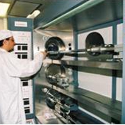
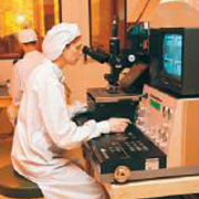
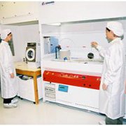
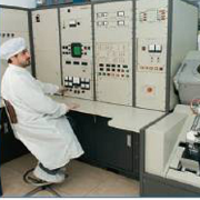
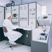
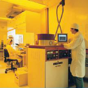
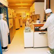
| Lithography and plasma etching are used as enabling fabrication technologies not only for traditional sectors, such as electronics and MEMs, but also for microfluidics, microarrays and lab-on-a-chip. We aim in developing deterministic and stochastic microfabrication processes for a broad range of applications including life sciences using top-down fabrication as well as plasma directed assembly:
- For nano-electronics using e-beam and Double Exposure 193nm lithography, our work focuses on Line Edge Roughness (LER) prediction using molecular simulation. We have combined our plasma simulation and lithography expertise to predict the LER transfer during plasma etching (see section A).
- For microfluidics, we use Deep Plasma Etching to fabricate PDMS, PMMA, PEEK and Si microfluidic devices. We demonstrated “smart” microfluidics incorporating capillary pumping and hydrophobic valving using our “plasma toolbox” technology. We also fabricated on chip affinity chromatography columns using TiO2 as stationary phase for phosphopeptide separations (see section B).
- In addition using our plasma processes for stochastic nano-texturing of polymers, we demonstrated high density protein microarrays both on PDMS and on PMMA, with almost 10fold higher binding capacity of proteins, and 100fold increased sensitivity compared to flat substrates. We have also optimized novel self aligned processes for protein microarrays on prepatterned substrates (see section B).
- We unveiled the mechanisms of plasma nanotexturing and identified the plasma reactor wall as the major factor for nanotexturing. In addition we have devised two methods to produce dual scale roughness on surfaces for control of wetting properties from hydrophilic, to hydrophobic, to oleophobic (see section C). Finally, we have discovered that plasma directed assembly of periodic nanodots can take place during etching of polymers, thus paving the way to plasma based lithography-less nanofabrication.
- In order to understand the phenomena of plasma nanotexturing and organization we are also doing Monte Carlo Simulation of plasma surface interactions (see section D).
Funding:
- EU NMP2 STREP Nanoplasma, Contract No 016424, 1/4/2006-31/3/2009
- GSRT, PENED 03 ED 202, 1/12/2005-30/06/2009
- MD3, IT 214948, 1/12/2007-30/11/2009
- SPAM, Marie Curie-ITN, Contract No 215723
|