• An Image Slideshow
  • An Image Slideshow
  • An Image Slideshow
  • An Image Slideshow
  • An Image Slideshow
  • An Image Slideshow
  • An Image Slideshow
May 2024
S M T W T F S
28 29 30 1 2 3 4
5 6 7 8 9 10 11
12 13 14 15 16 17 18
19 20 21 22 23 24 25
26 27 28 29 30 31 1
Nanotechnology and Mems Laboratory. Access Provided.

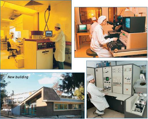
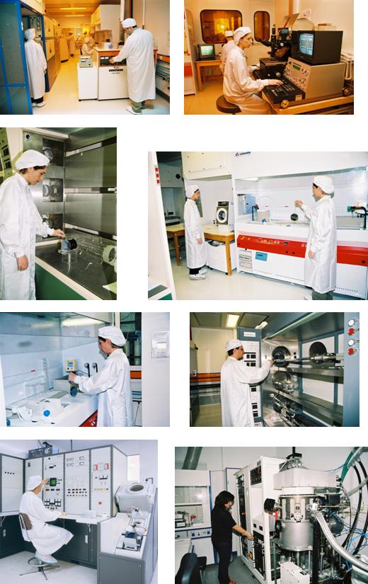
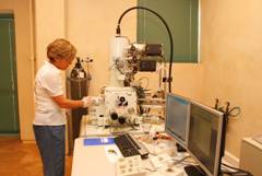
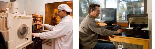
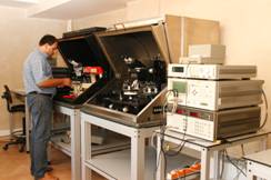
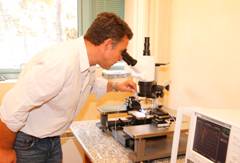
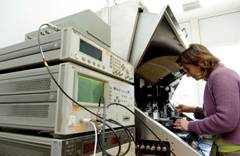
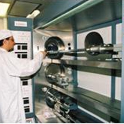
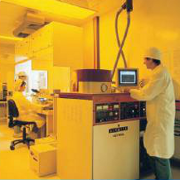
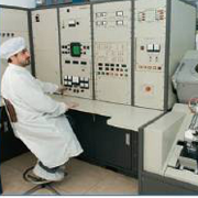
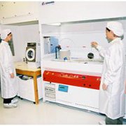
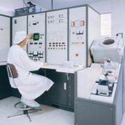
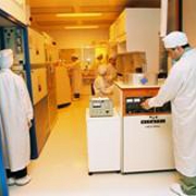
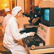
NANOTECHNOLOGY AND MEMS LABORATORY. ACCESS PROVIDED

The facilities and equipment of IMEL include a full silicon processing laboratory in a clean room area, equipped with lithography (optical, e- beam) and etching tools, thermal and chemical processing facilities, ion implantation, deposition of metals, dielectrics and poly- nanocrystalline silicon by physical and chemical processes (LPCVD, sputtering, e-gun and thermal evaporation), and process inspection equipment. The clean room is class 100 in the lithography area and class 1000 in the other areas. Satellite laboratories include electrical and optical characterization, micromachining and packaging laboratory, resist development laboratory, electron microscopy (SEM, STM/AFM), sensor characterization and testing equipment.

A new building of the Institute has been constructed in 2006 to host the electrical, optical and structural characterization laboratories. A photograph of the building is shown below.

The laboratory is certified under ISO 9001:2000 (Si processing and electrical characterizartion) and under ISO 17025:2005 (electrical measurements).

The equipment available and the expertise and competences include the following:

ACCESS PROVIDED

Access is provided in Si processing and Electrical and Optical characterization.
The access to IMEL’s infrastructure is financially supported by the IST-I3 European Project ANNA (for more details please visit: www.i3-anna.org)

MANAGEMANT OF THE ACCESS PROVIDED
The visitors are supported by IMEL’s staff in both measurements and interpretation of their results. Test structures for electrical characterization are fabricated by IMEL’s staff in the silicon processing facility.

IMEL offers also to visitors:

  1. Access to guest rooms and facilities
  2. Training
  3. Modern infrastructure e.g. library, computer and electronic services
  4. Training, scientific and technical support for using the infrastructure
  5. Support for the evaluation of their results
  6. Logistic support


  Home
About IMEL
Organisation
Location
Contact
Research
Micro and Nanofabrication Sensors and MEMs
R&D Projects
   EU Projects
   National Projects

Publications
Journal Papers
Conference Papers
Annual Reports
Patents
PhD & Master Theses

People
Researchers
Facilities & Services
Minasys - Center of Excellence
Nanotechnology and MEMS laboratory
   Lab 1
   Lab 2
   Lab 3
   Lab 4
Software
Education
PhD
Master Courses
Training
How to apply
News & Events
Research highlights
Awards & Distinctions
Events
   Conferences & Workshops
   Lectures
   Schools & Seminars
   Past Events
Job opening