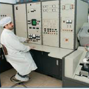
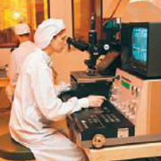
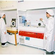
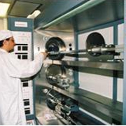
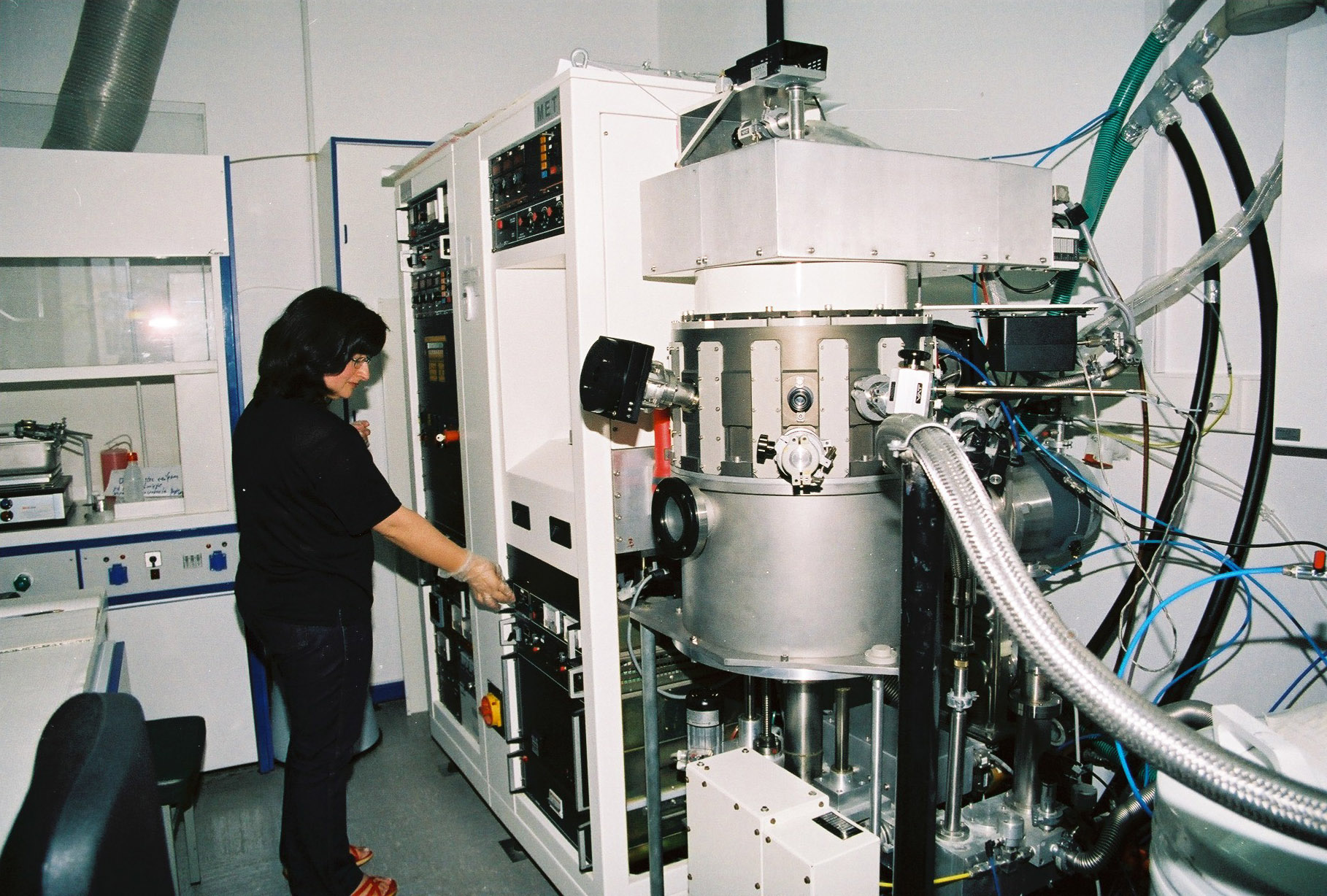
| The facilities and equipment of IMEL include a full silicon processing laboratory in a clean room area, complemented by characterization laboratories (electrical, optical, structural), micromachining and packaging equipment, resist development laboratory, as well as testing facilities and design, modeling and simulation tools. The clean room is equipped with lithography (optical, e- beam) and etching tools, thermal and chemical processing, ion implantation, deposition of metals, dielectrics and poly- nanocrystalline silicon by physical and chemical processes (LPCVD, sputtering, e-gun and thermal evaporation), and process inspection equipment.
|
|
|
|
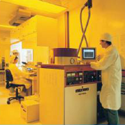
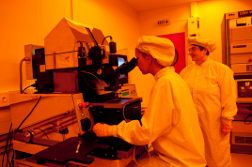
Lithography equipment
|
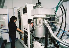
High density plasma etcher |
|
|
|
|
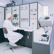
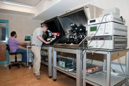
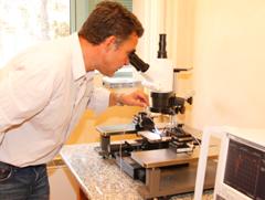
Electrical characterization equipment
|
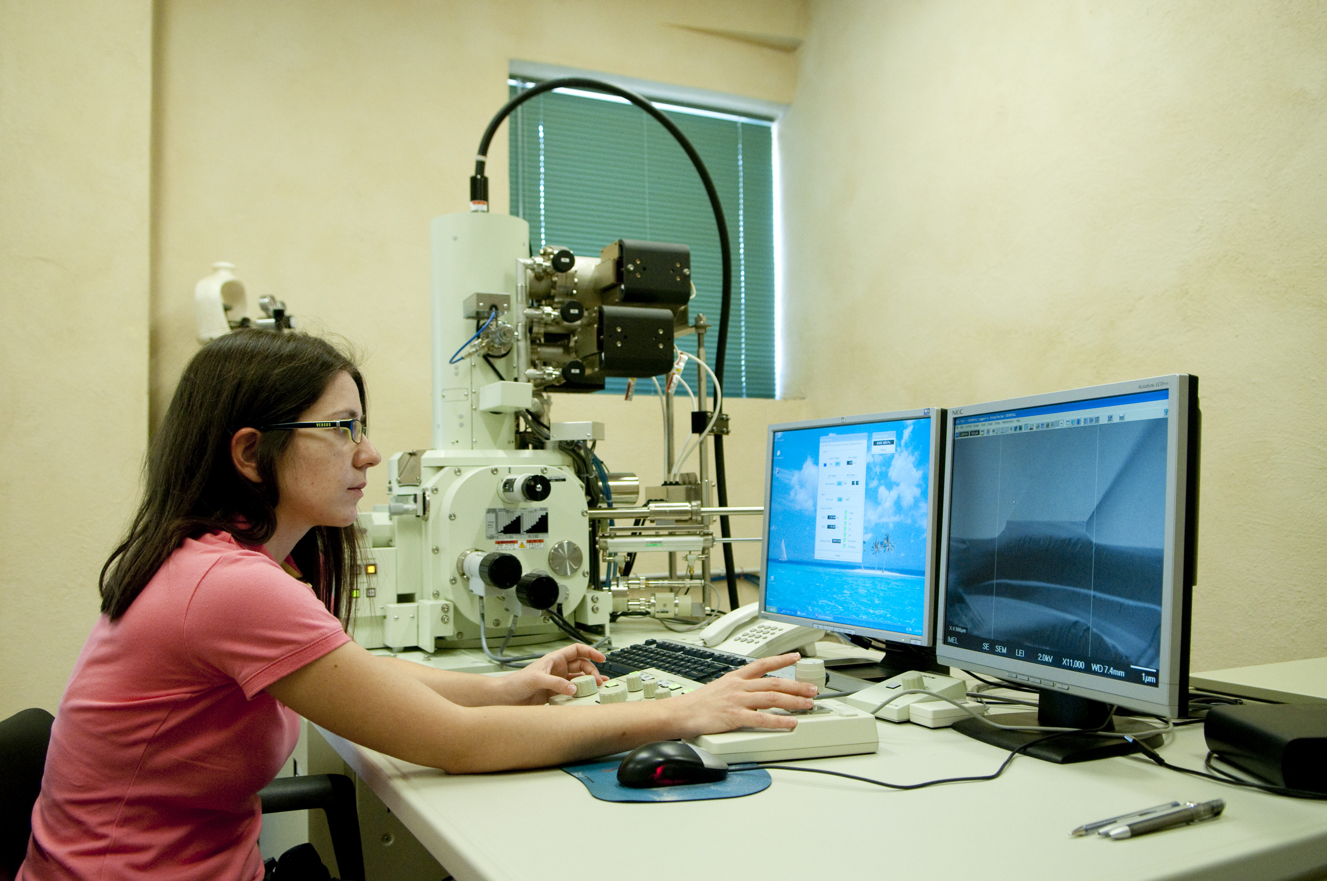
FEG SEM JEOL JSM-7401F |
|
|
|
|
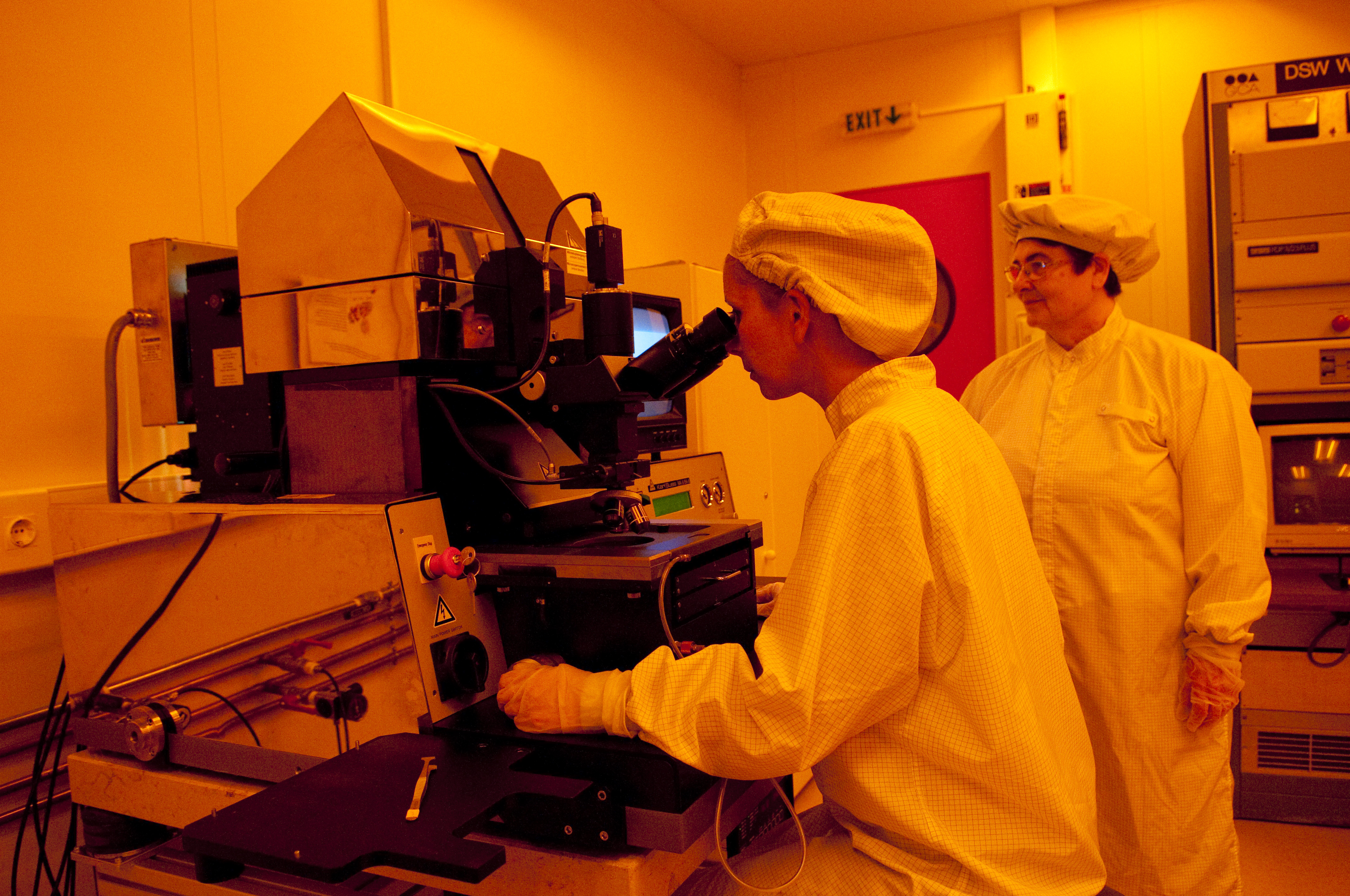
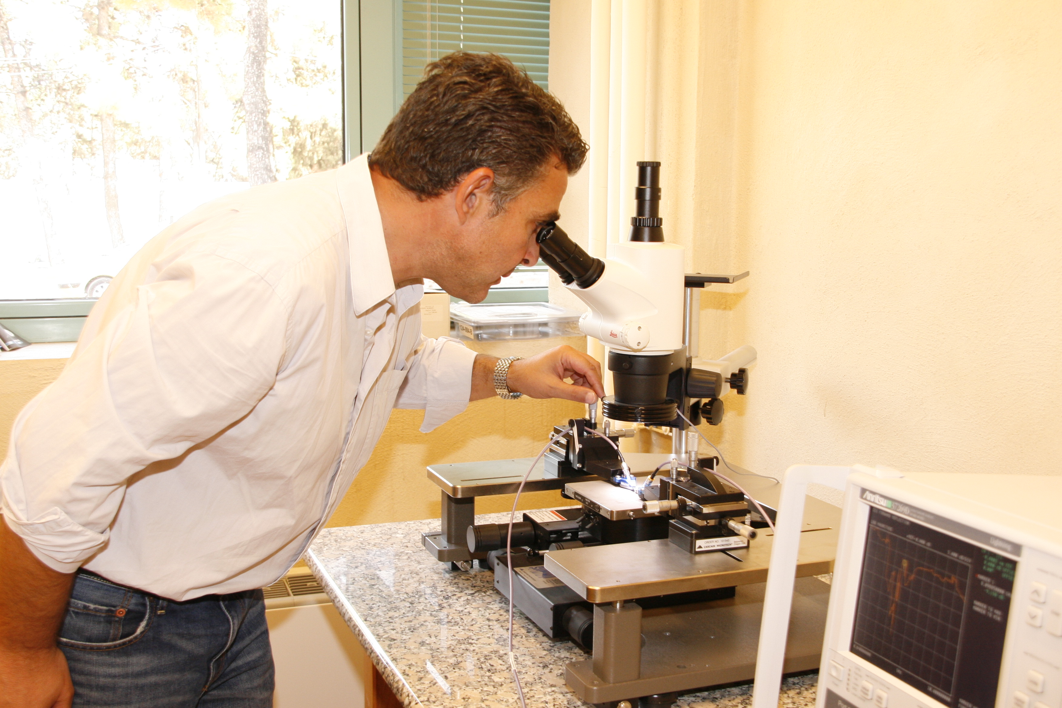
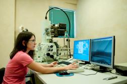
RF probe station
|
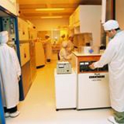
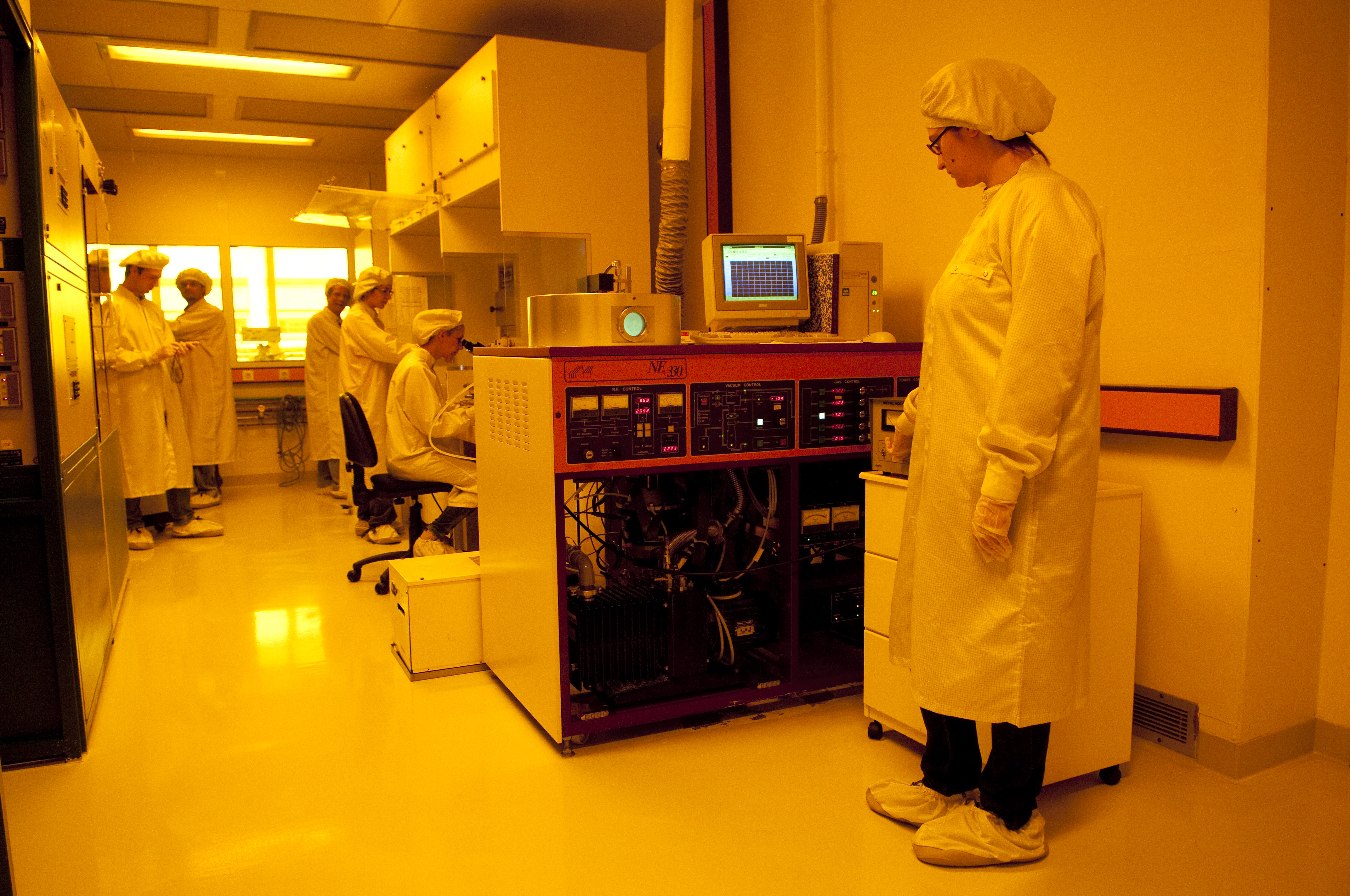
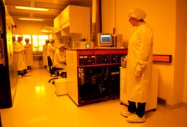
Lithography and etching area |
|
|
|
|
|
|
|