Focus
- Development of nano-scale fabrication technology.
- Fabrication of single electron transistors and single electron memories.
|
| Results and Accomplishments |
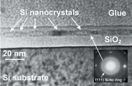
In collaboration with Sulford University two-dimensional arrays of
silicon nanocrystals (nc-Si) have been fabricated in thermally grown SiO2 films
by 1 keV 28Si+ ion implantation and subsequent thermal annealing.
The nanocrystals are located at a tunneling distance from the oxide
surface and/or the SiO2/Si interface. With increasing size, the nanocrystals
change from quasi-spheres to faceted platelets.
By reducing the implantation dose and the annealing temperature, the
size of the nanocrystals decreases, their size distribution becomes more narrow and their
spatial arrangement remains two dimensional.
|
|
|
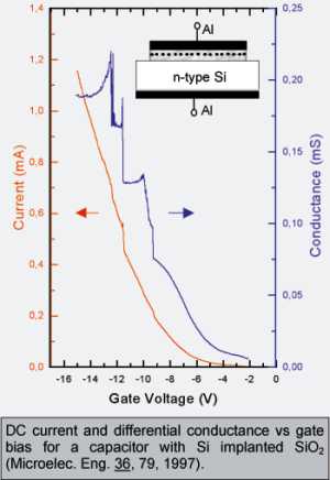
- Resonant tunneling via Si-nanocrystal quantum confinement in Al/SiO2/nc-Si/SiO2/Si
structures.
Electrical properties of Al/SiO2/nc-Si/SiO2/Si
structures have been investigated using dynamic conductance and dc-current measurements.
Resonant tunneling through these double barrier structures and Coulomb blockade effect due
to the accumulation of quantized charge in the silicon nanocrystals have been observed at
room temperature.
|
|
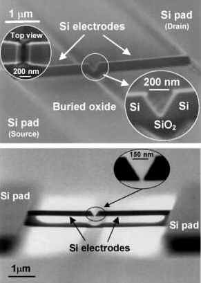
- Fabrication of Si electrodes with nano-scale separation using
photolithography and anisotropic etching
This study is prompted by the concept of a Single-Electron-Transistor that could be
fabricated on silicon-on-insulator (SOI) material using conventional silicon technology.
Nanometer-scale separation between the source and drain electrodes on the surface of the
buried oxide has been achieved by anisotropic etching of the silicon overlayer in an area
initially defined by optical lithography. This process is combined with very-low energy
implantation of Si and subsequent thermal annealing that results in the formation of Si
nanocrystals close to the surface of the buried oxide and it constitutes the basis of the
SET structures currently investigated at IMEL.
|
|
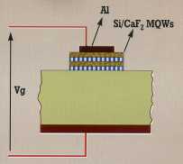
- Resonant tunneling at high electric fields in nanocrystalline (Si/CaF2)
multiquantum wells (MQWs)
|
|
In collaboration with CRMC2/CNRS , University of Maseille,
France, multi quantum wells were studied. The structures were deposited on silicon by MBE
at room temperature. A simple device as shown in the figure, composed of the mesa
structure, am aluminun gate and a back ohmic contact was used in order to study vertical
transport through the layers. Reions of negative differential resistance were observed in
the current-voltage characteristics at room temperature, attributed to resonant tunneling.
Electroluminescence in the visible range at room temperature was also obtained from these
structures. |