Focus
- Fabrication of Si quantum wires for light emission studies
- Deposition and characterization of nanocrystalline Si on SiO2 thin films or
nc-Si/SiO2 multilayers on Si for light emission studies
- Light emitting devices based on silicon quantum wires and dots in an SiO2
matrix
- Light emitting devices based on nanocrystalline on Si substrate (Si/CaF2)
multiquantum wells
- Integration of the above devices on Si with Si-based wave-guieds and detectors.
- Integration of GaAs based light emitting devices on Si by using the wafer fusion
technique.
-
|
|
|
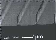
2-D Silicon structures fabricated by
lithography and highly anisotropic etching |
| Results and Accomplishments
|
| The following worldwide original results were obtained within
this activity: |
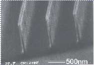
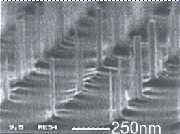
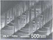
- A highly anisotropic silicon reactive ion etching process has been developed, based on a
mixture of SF6/CF3 gases. Compared to the currently used chlorine
chemistry, the above gases are environmentally friendly, and they are not corrosive. This
process permits to etch silicon down to dimensions in the nanometer scale. It was used to
fabricate silicon quantum wires of diameter 40-60 Å .
|
|
|
SEM images of silicon nanopilars
produced by lithography and highly anisotropic RIE
|
- Light emitting devices were fabricated based on silicon quantum wires obtained by
lithography and etching. These devices open important new possibilities in silicon
integrated optoelectonics.
- Light emitting devices based on nanocrystalline Si on very thin SiO2 layers
have been fabricated. Compared to porous silicon their main advantage is their stability
with time. Intense room temperature light emission in the visible and near IR range was
obtained.
- Light emitting devices based on nanocrystalline (Si/CaF2) MQWs were
developed.
|
|
|