The objectives of the project include:
a. Creation of a SiNW technology platform in Greece,
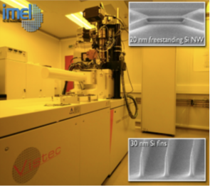
b. Development of JL SiNW FETs in tri-gate (TG) and gate-all-around (GAA) architectures based on top-down technology. Such activities will benefit of the electron-beam lithography tool (Vistec EBPG5000plusES) recently acquired by the Dept of Microelectronics of NCSR “Demokritos”, which allows the generation of sub-10nm features up to 150mm Si wafer,
c. LPCVD- and ALD-assisted development of trilayer dielectric stacks using nitride materials as charge storage medium,
d. Development of single- and multiple-bit charge-trapping SiNW memories in the form of TG and GAA JL SiNW FETs.